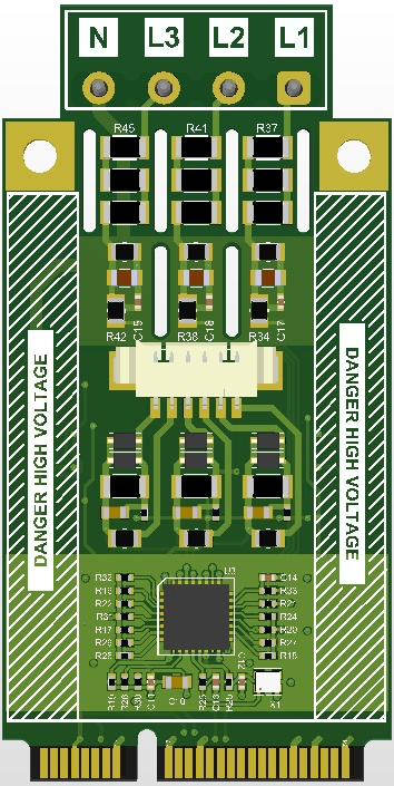
B202AA-PCIe: Three-Phase Energy Analyzer Module

I designed B202AA-PCIe as a high-precision measurement platform for industrial-level energy monitoring systems. At the heart of the module is the Analog Devices (Maxim Integrated) MAX78630 polyphase energy measurement IC. This IC can perform measurements at 0.1% class accuracy level in compliance with IEC 62053-21, IEC 62053-22 and IEC 62053-23 standards - meaning the performance class used in professional energy meters.

The reason I chose the Mini PCIe form factor in the design is that it provides both compact size and easy integration into existing systems. The project is completely open source: I share all design files including schematics, PCB files, BOM and software libraries.

High Voltage Warning - Risk of Death

This module operates with high voltage in the 85V-265V AC range. Improper use or inadequate isolation can lead to FATAL ELECTRIC SHOCK risk.

Safety Precautions:

  • Always disconnect electrical power when working on the module
  • Installation should only be performed by qualified and trained personnel
  • Do not measure or test on live circuits
  • Place the module in a properly insulated enclosure
  • Isolate all connection points that may be exposed to dangerous voltages
  • Act in accordance with national and international electrical safety standards

Disclaimer: This open source hardware project is for educational and development purposes. The developer cannot be held responsible for loss of life, property and equipment resulting from use. All responsibility belongs to the user.

Schematic Drawing

You can access the detailed schematic drawings of this module via the link below:

B202AA-PCIe Schematic File (PDF)


Hardware Architecture

B202AA-PCIe General System Block Diagram

The block diagram on page 1 of the B202AA-PCIe module clearly separates three main areas:

  • Field (high voltage) side
  • Isolated measurement and processing layer
  • Host / carrier board (low voltage) side

This structure makes it easier to understand how the board is positioned in terms of both electrical safety and system architecture.

1. Field Side (High Voltage Area)

On the left side of the block diagram are the field components connected to the grid:

  • Three-phase AC inputs: VR, VS, VT
  • Current transformers (CT_R, CT_S, CT_T): Isolate and scale line currents
  • Phase voltage sensing points: Taking phase-to-neutral or phase-to-phase voltage onto the board

Since this area includes all connections operating directly at 85-265 V AC and above, HV/LV separation and creepage/clearance rules are critical in the design.

2. Isolated Measurement and Processing Layer

The middle part of the block diagram shows the actual analog-digital measurement core on the board:

  • Voltage divider layer:
    The high voltage coming from VR-VS-VT lines is scaled to MAX78630's ±250 mV input range with a three-channel precision resistor network and RC filters.

  • Current transformer input layer:
    Signals from CST-1005 current transformers are processed with 24.9 Ω Kelvin burden, 10 Ω series resistor and BAS316 protection diodes and applied to MAX78630 current inputs.

  • MAX78630 energy measurement processor:
    Samples three-phase current and voltage information, performs RMS-active-reactive-apparent power and energy calculations internally.

  • Alarm isolation layer (AL1 / AL2):
    MAX78630's ISO_AL1 / ISO_AL2 lines are transferred to both LEDs on the board and AL1 / AL2 pins on the host side via TLP2362 optocouplers.

  • Phase voltage sense isolation layer (R / S / T):
    POVR / POVS / POVT signals generated in the internal measurement domain are transferred to SENSE_VR / SENSE_VS / SENSE_VT lines through analog isolation blocks.

This entire area is powered by 3V3ISO / GNDISO and is electrically isolated from the rest of the board.

3. Host / Carrier Board Side

On the right side of the block diagram is the host/carrier system that communicates with the board via the Mini PCIe socket:

  • 3.3 V and GND: Basic power supply provided by the host
  • UART interface: Exchange of measurement data and configuration commands via 3V3_UART_TX / 3V3_UART_RX lines
  • AL1 / AL2 alarm inputs: Hardware-level monitoring of critical situations in the field
  • SENSE_VR / SENSE_VS / SENSE_VT analog inputs: Monitoring of phase voltage magnitudes by external ADC or control systems
  • 3V3_POWER_EN: Power enable line that activates the isolated measurement block

The host side does not directly contact the grid; it only sees isolated signal and power lines.

4. Isolated UART and Power Block

Between the field and host side is the UART isolation and isolated power block shown as a separate layer in the block diagram:

  • ISOW7821-based isolation:
    Provides full galvanic isolation between 3V3_UART_TX / RX ↔ ISO_UART_TX / RX.
  • Integrated DC-DC converter:
    Produces isolated 3V3ISO supply for the measurement side from 3.3 V coming from the host.
  • Y2 class capacitor and ferrite beads:
    Used for EMC and common mode noise control.

This block is the only bridge between the board's "HV domain" and "LV domain", keeping all data and power flow under control.

5. Reference to Subsections

The subheadings under this block diagram explain each part of the architecture in detail:

  • Mini PCIe Socket and Card Edge Interface → Host side connections
  • Voltage Input and Divider Circuit → Phase voltage measurement chain
  • Current Transformer Inputs and Measurement Circuit → Phase current measurement chain
  • MAX78630 Measurement IC and UART Communication Architecture → Measurement core
  • Alarm Outputs and Optical Isolation (AL1 / AL2) → Hardware alarm architecture
  • UART Isolation Circuit and Isolated 3.3V Supply → Communication and power isolation
  • Phase Voltage Sense Isolation Layer (R / S / T) → External analog phase voltage outputs

In this way, when the reader looks at the block diagram on page 1, they can see the overall operation of the board at a glance; in the following sections, they can access the circuit-level details of each block.


Mini PCIe Socket

Mini PCIe Card Edge Connector

B202AA-PCIe, as the name suggests, is a board in Mini PCI Express form factor; however, it does not use PCIe data lines (TX/RX differential pairs) on it. The connector is mainly used in this project as a mechanical and electrical interface for:

  • 3.3 V power supply and GND distribution,
  • UART communication,
  • Alarm outputs (AL1 / AL2),
  • Phase voltage sense lines (SENSE_VR / SENSE_VS / SENSE_VT)

Therefore, B202AA-PCIe is not a PCIe peripheral card in the classical sense, but an isolated energy measurement module that uses the Mini PCIe connector as a carrier interface.

Signal Groups

The following signal groups are carried outside the board in the Mini PCIe socket on page 2 of the schematic:

  • Power and ground:
    • 3V3 – Main power supply of the board, provided by the host.
    • GND – Common reference ground.
    • Multiple power and ground pins are distributed in parallel in accordance with the Mini PCIe standard.
  • UART communication:
    • 3V3_UART_RX – Host's TX line (data coming to the board).
    • 3V3_UART_TX – Host's RX line (data leaving the board).
    • These lines correspond to ISO_UART_RX / ISO_UART_TX lines on the isolated side.
  • Power enable:
    • 3V3_POWER_EN – Control line that enables the board's isolated power block and measurement layer.
    • Works active HIGH; when the host pulls this line to 3.3 V level, isolation and VISO_3V3 production is activated.
  • Alarm lines:
    • AL1, AL2 – Active-LOW alarm outputs; isolated via optocoupler and can be used as both digital input and LED indicator.
  • Phase voltage sense lines:
    • SENSE_VR, SENSE_VS, SENSE_VT
      Coming from Phase Sense Isolation blocks on pages 3-5 and are isolated analog voltage references that can be read by the host ADC.

Host Side Perspective

The host or carrier board communicates with B202AA-PCIe via the Mini PCIe slot as follows:

  • Provides 3.3 V and GND to power the board.
  • Uses UART interface to receive measurement results.
  • Can read AL1 / AL2 signals to monitor critical events.
  • Can evaluate SENSE_VR / VS / VT lines to monitor phase voltage magnitude with its own ADC.

Thanks to this structure, the Mini PCIe socket serves as a compact and standard interface that enables plug-and-play integration of the B202AA-PCIe module into different systems without the need for complex PCIe protocols.


Voltage Input and Divider Circuit

Voltage Divider

I designed a precision voltage divider network to scale the high AC voltages (85-265 V RMS) on the VR-VS-VT phase lines to MAX78630's ±250 mV input range. In this divider, I used high-precision resistors with %0.1 tolerance and a two-stage RC filter structure - critical for both accuracy and frequency compensation.

Design Details

The voltage divider for each phase is configured as follows:

Resistor network:

  • Upper leg: 3× 1.1 MΩ series (R34, R35, R36) → Total 3.3 MΩ
    → %0.1 tolerance, 1206 SMD package (for high voltage isolation)
  • Series protection: 100 Ω (R37)
    → Transient protection and filter stability
  • Lower leg (reference): 1 kΩ (R46)
    → Compatible with ADC input impedance

RC filter stages:

  • 22 nF (C15-C17): For 50 Hz phase compensation
  • 1 nF (C18-C20): High frequency harmonic filtering

In PCB layout, I paid attention to HV-LV area separation: I applied a minimum 6 mm clearance and creepage distance between high voltage components and the low voltage side.

Division Ratio Calculation

From the classical voltage divider formula:

Vout = Vin × (Rlower / Rtotal)

Rtotal = 3,300,000 + 100 + 1,000 = 3,301,100 Ω
Division factor = 1,000 / 3,301,100 ≈ 0.0003029

Result: Vout ≈ Vin × 0.000303

Practical example:

  • 230 V RMS input → 230 × √2 × 0.000303 ≈ 98.5 mV (peak)
  • 400 V RMS input → 400 × √2 × 0.000303 ≈ 171 mV (peak)

Considering MAX78630's ±250 mV peak limit, this design can measure up to 584 V RMS - meaning there is a 45% safety margin in 400 V nominal systems.

Measurement Range and Safety Margin

Input VoltagePeak VoltageADC InputADC Usage
230 V RMS325 V98.5 mV39%
400 V RMS565 V171 mV68%
471 V RMS667 V202 mV81%
584 V RMS (max)826 V250 mV100%

I left a 45% safety margin for 400 V nominal systems in the design. In this way, transients or short-term overvoltages can be measured without saturating the ADC.

Frequency Compensation and Filter Design

I designed the RC filter structure in two stages:

First stage (22 nF):

  • Cutoff frequency: fc = 1 / (2π × 3.3 MΩ × 22 nF) ≈ 2.2 Hz
  • Phase shift at 50 Hz: -0.40° (from schematic analysis)
  • Purpose: Minimum phase error at fundamental frequency (50/60 Hz)

Second stage (1 nF + 100 Ω):

  • For filtering high frequency harmonics (3rd, 5th, 7th harmonics)
  • ADC input protection against sharp transients
  • 100 Ω series resistor also provides burden stability

With this structure, power measurement error (at PF=0.5) is -1.21% before compensation, < 0.05% after compensation.

Safety and PCB Layout
  • ≥6 mm creepage/clearance is applied between HV-LV regions.
  • Resistors are %0.1 tolerance; provides long-term gain stability.
  • Upper resistor network is 1206 package, providing high surface insulation.

Performance Summary

DescriptionValue
Maximum RMS Input Voltage584 V RMS
Maximum ADC Input±250 mV
Initial Gain Error±0.14 %
Phase Shift (50 Hz)−0.40°
Power Error (PF = 0.5, uncompensated)−1.21 %
Power Error (After Compensation)< 0.05 %
Long Term Gain Stability±0.2 %
Safety Margin in 400 V RMS System≈ 45 %

With this correction, the voltage divider documentation is fully compatible with the actual circuit design and schematic calculations in B202AA-PCIe hardware.


Current Transformer Inputs and Measurement Circuit

Current Transformer Inputs

In the B202AA-PCIe module, IR / IS / IT current channels are measured using one current transformer (CT) per phase. Each CT channel has a compact input stage consisting of a Kelvin-connected burden resistor, protection diodes and a small RC filter.

On the energy input connector, CT terminals are grouped as follows:

  • CT_R+ / CT_R− → R phase
  • CT_S+ / CT_S− → S phase
  • CT_T+ / CT_T− → T phase

These terminals are directly connected to the secondary of the current transformer and transmitted to the measurement circuit.

Selected Current Transformer (CST-1005)

In this design, Triad Magnetics CST-1005 series current transformers are used for each phase. The basic features of this component:

  • Model: CST-1005 (CST1005)
  • Manufacturer: Triad Magnetics
  • Current ratio: 5 A : 5 mA (1000:1)
  • Secondary DC resistance: 40 Ω
  • Recommended burden resistor (datasheet): 100 Ω
  • Operating frequency range: 50-60 Hz
  • Dielectric withstand: 4 kV
  • Accuracy: ±3 % (in 2 A - 20 A range)

The datasheet specifies 0.0958 V/A output voltage for 100 Ω burden resistor. In this design, by using 24.9 Ω burden:

  • Voltage/current ratio is pulled to approximately 0.0239 V/A level
  • Approximately 0.12-0.125 V_RMS output voltage is obtained at nominal 5 A current

These values are consistent with the burden and scaling calculations given below.

Design Architecture

The input structure for each phase current channel follows a common architecture:

  • Series input resistor: 10 Ω, %0.1, 0805 (R7, R10, R13)
  • Burden (load) resistor: 24.9 Ω, %0.1, 1/4 W, 1206 (R8, R11, R14)
  • Burden capacitor: 470 pF, 50 V, 0603 (C7, C8, C9)
  • Protection diodes: BAS316, SOD-323, anti-parallel (D3-D8)

The burden resistor is connected with Kelvin Connection as indicated in the schematic. In this way, the additional resistance of the printed circuit board traces and solder joints does not affect the measurement gain; MAX78630 only sees the actual voltage across the burden.

Burden and Scaling

The design is scaled for 5 A nominal and 7 A maximum line current. The CT ratio is designed to be 1000:1 (5 A → 5 mA, Triad Magnetics CST-1005).

Nominal value:

I_sec = 5 A_RMS / 1000 ≈ 5 mA_RMS
V_burden = 5 mA × 24.9 Ω ≈ 0.125 V_RMS (0.177 V_peak)

According to the values in the schematic:

  • Nominal current (5 A RMS): 0.125 V_RMS → 0.177 V_peak
  • Maximum current (7 A RMS): 0.174 V_RMS → 0.246 V_peak
  • MAX78630 input limit: ±250 mV_peak

This structure uses approximately 98% of the ADC full scale range and provides high-precision current measurement.

Burden power:

P = V² / R ≈ (0.174 V_RMS)² / 24.9 Ω < 2 mW

Protection and Safety

In case the CT secondary is open circuit, the voltage can rise to hundreds of volts. Therefore, on each channel:

  • Two anti-parallel BAS316 diodes are connected across the burden resistor.
  • Normally, since the voltage across the burden is at ±0.25 V_peak level, the diodes do not conduct.
  • In case of a possible open circuit, the diodes conduct at ±0.7 V level, limiting the secondary voltage to a safe level.

Additional safety elements:

  • 470 pF capacitor filters high frequency noise.
  • 10 Ω series resistor protects the circuit by limiting the current when the protection diodes conduct.

Performance Summary

DescriptionValue
Nominal Line Current5 A RMS
Maximum Line Current7 A RMS
CT Ratio1000:1 (Triad CST-1005)
Burden Resistor24.9 Ω, %0.1, 1/4 W
MAX78630 Current Input Limit±250 mV_peak
Nominal Burden Voltage0.125 V_RMS (0.177 V_peak)
Maximum Burden Voltage0.174 V_RMS (0.246 V_peak)
Used ADC Range≈ %98
Burden Power Loss< 2 mW
Protection ElementsBAS316 anti-parallel diode pair + 470 pF filter

This current input topology ensures safe operation of the CTs while achieving signal levels close to full scale for MAX78630.


MAX78630 Measurement IC and UART Communication Architecture

MAX78630 SOC Core Schematic

At the heart of the B202AA-PCIe module is the MAX78630+PPM energy measurement processor that processes three-phase voltage and current information in real time. This IC samples phase voltage (Analog_VR, Analog_VS, Analog_VT) and current (Analog_IR, Analog_IS, Analog_IT) signals, performs power and energy calculations with its internal DSP engine, and transmits the result to the upper system via isolated UART interface.

Analog Measurement Inputs

The analog side of MAX78630 is directly connected to the voltage dividers and current transformer input circuits explained in the previous sections:

  • Phase voltages: Analog_VR, Analog_VS, Analog_VT
  • Phase currents: Analog_IR, Analog_IS, Analog_IT

These signals:

  • For voltage channels: high impedance voltage divider + RC filter
  • For current channels: CST-1005 current transformer + burden + diode protection + RC filter

are connected to MAX78630's differential ADC inputs (AVx / AIx) via. In this way, the entire measurement chain produces low-noise signals scaled to ±250 mVpeak full scale range.

Reference and Oscillator Structure

MAX78630 is supported by external reference and clock components for proper operation of its internal delta-sigma ADC and DSP core:

  • Reference voltage (VREF) is filtered with closely placed bypass capacitors and isolated from analog/digital noise.
  • 32.768 kHz crystal is connected to XIN/XOUT pins to create the measurement time base. This clock:
    • Sampling rate,
    • Frequency calculation,
    • Is a critical component that determines long-term energy integration accuracy.

This structure is set up with typical connections in accordance with manufacturer application notes.

UART Interface and Isolation

B202AA-PCIe establishes communication between MAX78630 and the main system via UART. In the schematic:

  • Serial lines on the IC side: ISO_UART_RX / ISO_UART_TX
  • Lines on the board edge (host) side: 3V3_UART_RX / 3V3_UART_TX
  • Between them is a digital isolation layer that separates these two sides.

The advantages of this architecture:

  • Prevents errors or transients on the high voltage side from passing to the host system.
  • Reduces ground loops and common mode noise.
  • Limits other digital circuits on the same board from injecting noise into the AC measurement side.

In accordance with the MAX78630 datasheet, the device is configured to communicate via UART. Although the IC actually supports SPI and I²C interfaces as well, in this design only the UART line is active; the project architecture is completely built around the UART protocol.

Addressing, Alarm and Control Lines

As shown in the block schematic, in addition to serial communication, the following digital lines are also open for use:

  • AL1 / AL2: Multi-purpose digital outputs that can be configured to carry alarm and status information within the IC. These lines are also isolated via ISO_AL1 / ISO_AL2.
  • ADDR0 / ADDR1 (even if net names are not visible in the schematic): Pins that allow device address selection when using multiple MAX78630s; in this design, they are defined with resistors to be a fixed address.
  • RESET / IRQ: Control lines designed to safely restart the IC and generate event-based interrupts (measurement ready, error, etc.).

Thanks to these lines, higher-level software can see error conditions, change measurement speed, and restart the IC in the field if necessary.

Power Topology

MAX78630 uses separated power domains for both measurement accuracy and EMC performance:

  • 3V3ISO: Isolated 3.3 V supply line; both MAX78630 and UART/ALARM isolation layer are powered from this line.
  • GNDISO: Reference ground belonging to the measurement side; physically and electrically separated from the rest of the board.
  • On the digital side, there is 3V3 and system GND line at the board edge connector.

This separation is designed in accordance with the classical HV/LV area separation principle, which is also emphasized in the block schematic with the "Serial Comm Isolation" section.

Thanks to this architecture, the measurement IC operates isolated and safely on the high voltage side; while the host side only sees the isolated UART line. In this way, both electrical safety and software integration are kept in a simple and repeatable structure.


Alarm Outputs and Optical Isolation (AL1 / AL2)

AL1 / AL2 Alarm Isolation Circuit

The AL1 and AL2 lines in the B202AA-PCIe module are transmitted to the host system via the optical isolation layer that carries MAX78630's ISO_AL1 / ISO_AL2 alarm outputs safely and noise-resistant to the AL1 / AL2 pins at the board edge.

Thanks to this structure:

  • The high voltage measurement area and the host side are galvanically separated,
  • Voltage pulses and ground potential differences that may come via alarm lines are not carried to the host system,
  • The same lines are used both for digital alarm signal and for visual monitoring with local LED indicator.

Circuit Architecture (AL1 / AL2 Common Structure)

Both alarm channels have the same topology:

  • Isolated side inputs/outputs: ISO_AL1 / ISO_AL2
  • Host side alarm pins: AL1 / AL2
  • Optical isolation: Toshiba TLP2362 high-speed digital optocoupler
  • Power supply:
    • Isolated side: 3V3ISO / GNDISO
    • Host side: 3V3 / GND

Basic components for each channel:

  • Optocoupler: TLP2362 (separate packages for AL1 and AL2)
  • Input current limiting resistor: 1.8 kΩ, 0402, 1/10 W (e.g. R2, R5)
  • Output series resistor: 47 Ω, 0402, 1/16 W (e.g. R3, R6)
  • Pull-up resistor: 4.7 kΩ, 0402, 1/16 W (e.g. R1, R4)
  • Alarm LED: Red SMD LED (D1 for AL1, D2 for AL2)
  • Supply bypass capacitors:
    • 100 nF, 6.3 V, 0402 (C1, C4)
    • 1 µF, 6.3 V, 0402 (C2, C5)
    • 47 nF, 6.3 V, 0402 (C3, C6)

Multiple bypass capacitors placed on both sides of the optocoupler suppress supply noise in accordance with manufacturer recommendations and ensure stable operation of the optical isolation layer.

Operating Principle and Logic Levels

According to the notes on the schematic, AL1 and AL2 outputs:

  • Work with Active LOW logic,
  • On the schematic:
    • ON = Alarm
    • OFF = No Alarm is defined as.

This means:

  • In normal condition (no alarm), the optocoupler output is not conducting, AL1 / AL2 lines are kept at 3.3 V level thanks to 4.7 kΩ pull-up and the LED is off.
  • When an alarm occurs, the optocoupler LED draws current on the ISO_AL1 / ISO_AL2 side, the output transistor conducts:
    • Pulls the AL1 / AL2 line to GND (LOW),
    • Creates a visual alarm indicator by flowing current through the red LED.

Thanks to this structure, the host side can directly read the AL1 / AL2 pins as open-collector / active-low alarm output.

Isolation and PCB Design Notes

The alarm isolation layer complies with the following rules together with other isolation areas on the same board:

  • Copper clearance between GNDISO and system GND should be designed to be at least 6 mm.
  • 100 nF and 1 µF bypass capacitors around the optocoupler should be placed as close to the package as possible.
  • Although both sides of the alarm circuits operate at 3.3 V level, thanks to optical isolation:
    • Potential differences between different ground references do not cause problems,
    • AL1 / AL2 lines going out to the external system with cable cannot carry noise back to the module's high voltage measurement area.

Usage Scenarios

These alarm lines are typically used for:

  • Overcurrent / overvoltage,
  • Phase loss or imbalance,
  • Internal error (e.g. MAX78630 fault condition),
  • Transmitting "alarm occurred" information to external relay or contactor drivers,

monitoring such situations.

On the host side, AL1 / AL2 lines:

  • As a pull-up compatible, active-low alarm input to a microcontroller GPIO input,
  • As an open-collector input that triggers an optocoupler on the PLC / digital input module side,

can be used directly.

In this way, B202AA-PCIe both safely exposes alarm information isolated on the measurement side to the outside world and provides fast visual diagnosis in the field with on-board LEDs.


UART Isolation Circuit and Isolated 3.3V Supply

UART Isolation Circuit

In the B202AA-PCIe module, serial communication between the high voltage measurement area where MAX78630 is located and the host system is provided via the UART isolation block. This block combines both digital data lines (TX/RX) and the isolated 3.3V supply needed by the measurement side around a single IC.

Basic Architecture

The UART isolation layer combines four main functions:

  • Digital isolation:
    • Host side: 3V3_UART_TX, 3V3_UART_RX
    • Isolated side: ISO_UART_TX, ISO_UART_RX
  • Isolated DC-DC converter:
    • Input: 3V3
    • Output: VISO_3V3
    • Isolated ground: GNDISO
  • Supply filtering and EMI suppression
  • Power activation control: 3V3_POWER_EN

Used IC: Texas Instruments ISOW7821

At the center of UART isolation is the Texas Instruments ISOW7821FDWE isolation IC. This IC:

  • Provides bidirectional digital isolation channels
  • Contains built-in isolated DC-DC converter
  • Makes the UART line safe with full isolation

Basic pin mappings:

  • Vcc / GND → primary 3.3V supply
  • VISO_3V3 / GNDISO → isolated 3.3V output
  • InA / OutA / InB / OutB → UART TX/RX lines
  • EN1 → controlled by 3V3_POWER_EN

Supply and Filtering Network

Multi-stage filtering in accordance with manufacturer recommendations is applied on both sides of ISOW7821:

Input side (3V3 – GND):

  • FB1: Ferrite bead (HF noise filtering)
  • C24, C27: 1 µF
  • C25, C26: 100 nF
  • C29: 2.2 µF

Isolated side (VISO_3V3 – GNDISO):

  • C28: 4.7 µF
  • Closely placed small capacitors increase DC-DC stability

Additionally, common mode noise is controlled with a Y2 class safety capacitor.

3V3_POWER_EN and Power Management

  • 3V3_POWER_EN works active HIGH
  • R75 (10 kΩ) keeps the line at a certain level
  • C28 smooths sudden current draws

In this way, the UART isolation block can only be activated when needed.

UART Lines and Resistor Network

  • R71-R74 (33 Ω): Signal line damping, EMI reduction
  • R67-R70 (47 kΩ): Pull-up resistors, ensure lines stay HIGH in idle state

This structure ensures the UART line remains stable even when the host is not connected.

Isolation Distances and PCB Rules

Around ISOW7821 in accordance with IPC9592 standard:

  • ≥ 6 mm creepage/clearance between isolated and non-isolated areas
  • The two sections are completely separated by copper clearances

Thanks to this structure, the host system only sees completely isolated UART signals and transient or error conditions in the high voltage field cannot be carried to the host side.


Phase Voltage Sense Isolation Layer (R / S / T)

Phase Sense Signal Isolation

In the B202AA-PCIe module, it is intended that the measured phase voltages (VR / VS / VT) are not only processed by MAX78630, but also presented to the host system as isolated analog "sense" signals when necessary. For this reason, the R / S / T Phase Sense Signal Isolation blocks on pages 3, 4 and 5 in the schematic have been designed. The structure is exactly the same for all three phases.

This isolation layer receives the POVR / POVS / POVT signals in the internal analog measurement domain and transmits them to the SENSE_VR / SENSE_VS / SENSE_VT pins at the board edge as safe, galvanically isolated analog signals.

Block Architecture and Net Structure

The naming of input-output lines for each phase is as follows:

  • Input (isolated measurement domain):
    • R Phase: POVR
    • S Phase: POVS
    • T Phase: POVT
  • Isolated output domain (host side differential signal):
    • POSENSE0VR / NLSENSE0VR
    • POSENSE0VS / NLSENSE0VS
    • POSENSE0VT / NLSENSE0VT
  • Mini PCIe board edge:
    • SENSE_VR, SENSE_VS, SENSE_VT

Thanks to this structure, the user can read phase voltages either differentially or with a single-ended reference.

Typical Flow Structure of One Phase (R Phase Example)

The structure used for R phase (page 3 — R Phase Sense Signal Isolation) follows these steps:

  1. The POVR signal coming from the internal measurement domain enters the isolation block.
  2. Galvanic isolation is applied via analog isolation circuit.
  3. POSENSE0VR / NLSENSE0VR differential pair is generated on the host side.
  4. This pair is routed to the SENSE_VR pin at the board edge.

For S and T phases, the same structure is repeated one-to-one as POVS → SENSE_VS and POVT → SENSE_VT.

Purpose and Usage Scenarios

This isolation layer is designed to meet the following needs:

  • Safe Phase Voltage Telemetry:
    The host system can safely monitor phase voltages without directly connecting to the grid voltage.

  • Galvanic Separation:
    Full electrical isolation is provided between the measurement domain and the host domain; transients or ground shifts cannot reach the host side.

  • Standard Analog Output:
    External ADC, controller or data acquisition systems can directly read SENSE_VR/VS/VT pins.

Bu kütüphane, gerçek sahada kullanılan projelerden gelen ihtiyaçlara göre sürekli gelişen bir açık kaynak projedir. Kullanıcı geri bildirimleri, yeni fonksiyonların eklenmesi ve mevcut yapının iyileştirilmesi açısından kritik öneme sahiptir.

Bu kütüphaneyi hem kişisel hem de ticari projelerinde özgürce kullanabilirsin. Herhangi bir lisans kısıtı uygulanmamaktadır; amacım, bu kütüphanenin mümkün olduğunca fazla gerçek dünya projesinde yer almasıdır. Özel bir entegrasyon ihtiyacın, ticari bir planın veya teknik bir sorunun varsa bana e‑posta üzerinden her zaman ulaşabilirsin: akkoyun@me.com Geri bildirimlerini veya kullanım senaryolarını paylaşman, projeyi geliştirmem açısından büyük katkı sağlar.