B182AA
B182AA-PCIe is an RS485 communication module designed in PCIe form factor.
Overview
B182AA-PCIe is designed to simplify integration by decoupling the RS485 layer from the main board in systems that require field communication. The module follows the qSlot mechanical approach and provides a reusable communication block across different products, helping teams move the same communication infrastructure to different hardware platforms faster.
For details about the qSlot architecture, visit the qSlot page.
How It Works
B182AA-PCIe is powered from the 3V3 rail and connected to the processor over a 3.3V UART interface. The module defaults to receive mode; in this state, data from the RS485 bus is forwarded to the processor through UART_RX.
When transmitting data on the RS485 line, the COMM_EN pin is driven HIGH to enable the driver stage, and data from UART_TX is placed on the RS485 bus. After transmission, COMM_EN is driven LOW to return the line to receive mode.
This control sequence ensures collision-free direction management on a half-duplex RS485 bus.
Technical Specifications
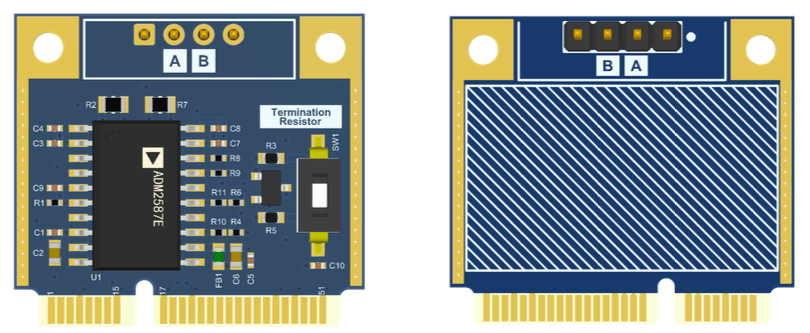
B182AA-PCIe is a qSlot-compatible RS485 communication module in PCIe form factor and uses a half-duplex communication topology. The main communication IC is Analog Devices ADM2587E, integrating the RS485 driver/receiver and isolation layer in a single package for improved robustness against field noise and ground potential differences.
The logic side is powered from 3V3, UART communication runs through UART_RX and UART_TX, and direction/enable control is handled by COMM_EN.
The RS485 physical interface is routed through RS485_A/RS485_B and RS485_Y/RS485_Z networks. External line protection is provided by SM712 (600W, dual-channel TVS/ESD), protecting the transceiver lines against ESD and surge events. The module targets 500 kbps communication speed and a 15 kV ESD robustness level.
Pinout Diagram
qSlot pin usage details. The B182AA module uses the communication lines below.
| Notes | Pin Name | Pin No | Pin No | Pin Name | Notes |
|---|---|---|---|---|---|
| High-current supply | POWER_FEED | 01 | 02 | POWER_FEED | High-current supply |
| High-current supply | POWER_FEED | 03 | 04 | POWER_FEED | High-current supply |
| High-current supply | POWER_FEED | 05 | 06 | POWER_FEED | High-current supply |
| 3V3 domain supply | 3V3 | 07 | 08 | 3V3 | 3V3 domain supply |
| Auxiliary supply | VCC | 09 | 10 | VCC | Auxiliary supply |
| USB D+ | USB D+ | 11 | 12 | PWR_EN | Power line enable |
| USB D- | USB D- | 13 | 14 | COMM_EN | RS485 TX enable |
| GND reference | GND | 15 | 16 | GND | Ground reference |
| KEY | KEY | ||||
| GND reference | GND | 15 | 16 | GND | Ground reference |
| UART1 Rx (Module Rx) | UART1 RX | 19 | 20 | UART RX | RS485 RX (Module Rx) |
| UART1 Tx (Module Tx) | UART1 TX | 21 | 22 | UART TX | RS485 TX (Module Tx) |
| GND reference | GND/AGND | 15 | 16 | GND | Ground reference |
| Analog 1 | ANALOG1 | 25 | 26 | DIO1 | Signal line 1 |
| Analog 2 | ANALOG2 | 27 | 28 | DIO2 | Signal line 2 |
| Analog 3 | ANALOG3 | 29 | 30 | DIO3 | Signal line 3 |
| Analog 4 | ANALOG4 | 31 | 32 | DIO4 | Signal line 4 |
| SPI communication | SPI_MOSI | 33 | 34 | DIO5 | Signal line 5 |
| SPI communication | SPI_MISO | 35 | 36 | DIO6 | Signal line 6 |
| SPI communication | SPI_SCK | 37 | 38 | DIO7 | Signal line 7 |
| SPI communication | SPI_CS | 39 | 40 | DIO8 | Signal line 8 |
| GND reference | GND | 15 | 16 | GND | Ground reference |
| PWM communication 1 | PWM1 | 43 | 44 | PWM2 | PWM communication 2 |
| GND reference | GND | 15 | 16 | GND | Ground reference |
| Sensor (I2C) Enable | PERIPH_EN | 47 | 48 | I2C_SCL | I2C Clock |
| Sensor (I2C) Int | PERIPH_INT | 49 | 50 | I2C_SDA | I2C Data |
| GND reference | GND | 51 | 52 | GND | Ground reference |
Onboard Settings and Indicators
The board includes a DIP switch for enabling/disabling the RS485 termination resistor. When the switch is ON, line termination is enabled; when the switch is OFF, termination is disabled. If the module is placed at the beginning or the end of the RS485 bus, termination should be enabled. If the module is not at the beginning or end of the bus and works as a middle node, termination must be disabled; otherwise, bus impedance is disturbed and communication quality can degrade.
Downloadable Resources
For all design files, schematics, and manufacturing outputs, visit the Github B182 repository.
Bu kütüphane, gerçek sahada kullanılan projelerden gelen ihtiyaçlara göre sürekli gelişen bir açık kaynak projedir. Kullanıcı geri bildirimleri, yeni fonksiyonların eklenmesi ve mevcut yapının iyileştirilmesi açısından kritik öneme sahiptir.
Bu kütüphaneyi hem kişisel hem de ticari projelerinde özgürce kullanabilirsin. Herhangi bir lisans kısıtı uygulanmamaktadır; amacım, bu kütüphanenin mümkün olduğunca fazla gerçek dünya projesinde yer almasıdır. Özel bir entegrasyon ihtiyacın, ticari bir planın veya teknik bir sorunun varsa bana e‑posta üzerinden her zaman ulaşabilirsin: akkoyun@me.com Geri bildirimlerini veya kullanım senaryolarını paylaşman, projeyi geliştirmem açısından büyük katkı sağlar.